Krypton Solutions Services: PCB Layout
Krypton’s PCB development team is ready to work with circuit and application experts to make your design a reality. Working side by side with your layout team, Krypton will receive real time input to reduce development schedules and unsure designs are completed to specifications. Your engineers are welcome to work with us here at Krypton, or we can deploy layout experts to your site.
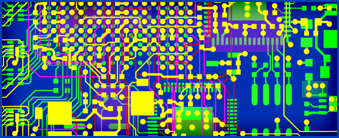
Krypton Solutions’ PCB layout experts can create your design of high complexity, high speed and high layer count boards. Our symbol and footprint services are offered as a standalone service, and a parallel service with PCB layout.
Our layout team stays up to date with the new technology and successfully integrates the latest PCB design practices. A list of some of the technologies implemented include:
Krypton Solutions Services: PCB Layout
- Microvia technology
- Blind and buried vias
- Buried capacitors and resistors
- Controlled impedance
- Symbol creation
- Footprint Creation
- High speed RF level design
- Up to 40 layer PCBs
- Flex and Rigid Flex PCBs
- CSP technology
Design Tools
The Hardware and PCB design teams use a number of schematic capture and PCB layout tools to capture and implement a printed circuit board design.
Schematic Capture
- Cadence
- Altium
Symbol & Footprint
- Cadence
- Altium
PCB Layout
- Cadence
- Altium
Signal Integrity
Signal Integrity is an important aspect of high speed PCB designs to verify expectations and requirements. As signal speeds continue to increase, relying on general PCB routing guidelines is becoming insufficient. Signal integrity analysis is quickly becoming required to help guarantee the quality of signals prior to building prototypes and verifying signal integrity in the lab.
Krypton Solutions has experienced developers that can utilize the following software tools for signal integrity analysis for specific customers based on their needs.
- Cadence SPECTRAQuest